
PHYS-131 · Lesson 11 of 12 · 29 min
Semiconductors, sensors and modern devices
Almost every electrical device built in the last fifty years depends on semiconductors: the diodes that convert AC to DC in every charger, the transistors that switch power in motor drives and compute in processors, the LEDs that light buildings and screens, the solar cells on roofs and the sensors that measure temperature, light, magnetic field and force in cars, phones and factories. This lesson connects the physics of the earlier lessons to these devices. It explains why semiconductors conduct as they do, how doping creates n-type and p-type material, and how a p-n junction becomes a diode, an LED or a solar cell. It then describes transistors as electronic switches, and a family of sensors that turn physical quantities into electrical signals. The aim is physical understanding; ELE and ENCM courses develop the electronics in detail.
Conductors, insulators and semiconductors
In a solid, electrons can only have energies within certain allowed bands. In a metal, the highest occupied band is only partly filled, so electrons can move into nearby empty states and conduct easily. In an insulator, the occupied valence band is full and separated from the empty conduction band by a large energy gap, several electronvolts, so almost no electrons can conduct. A semiconductor has a smaller band gap, 1.12 eV for silicon, 1.42 eV for gallium arsenide and 3.4 eV for gallium nitride, so at room temperature a few electrons are thermally excited across the gap, leaving behind holes, missing electrons that behave as positive charge carriers.
Pure silicon is a poor conductor, but its conductivity can be controlled precisely by doping, adding tiny amounts of other elements. Phosphorus, with five outer electrons to silicon's four, donates an extra electron: n-type silicon, with negative electrons as majority carriers. Boron, with three, accepts an electron, creating a hole: p-type silicon. A doping level of one atom in ten million raises the conductivity of silicon by a factor of thousands. Unlike metals, whose resistance rises with temperature (Lesson 5), intrinsic semiconductors conduct better when hot, because more carriers are excited across the gap, a property used in thermistors and a hazard in power electronics.
The band gap also sets how semiconductors interact with light (Lesson 10). A photon can lift an electron across the gap only if its energy hf exceeds the gap energy, so silicon absorbs light with wavelengths shorter than 1240/1.12 = 1110 nm and is transparent beyond, which is why silicon solar cells and camera sensors respond to visible and near-infrared light.
The p-n junction and the diode
Where p-type and n-type regions meet, electrons diffuse from the n side into the p side and holes the other way, recombining near the junction. This leaves a thin depletion region with no free carriers and a built-in electric field (about 0.7 V across it in silicon) that stops further diffusion. Applying a forward voltage, p side positive, reduces this barrier and current flows freely once the voltage exceeds about 0.6 to 0.7 V; applying a reverse voltage widens the barrier and only a tiny leakage current flows. The p-n junction is therefore a diode, a one-way valve for current, with a strongly nonlinear current-voltage characteristic:
where \(I_0\) is a tiny saturation current and n an ideality factor between 1 and 2. Diodes rectify AC to DC, protect circuits from reversed batteries, clamp voltage spikes (the flyback diodes of Lesson 8) and, as Zener diodes operated in reverse breakdown, regulate voltage.
Worked problem
A full-wave rectifier
A transformer delivers 12 V RMS to a bridge rectifier (four diodes, two conducting at a time, each dropping about 0.7 V) feeding a 4700 µF smoothing capacitor and a 1.0 A load. Estimate the DC output voltage and the ripple.
Show solution
- Peak transformer voltage: \(12\sqrt{2} = 17.0\) V; after two diode drops, 15.6 V.
- Full-wave rectification recharges the capacitor 120 times a second. Between peaks, the capacitor supplies the load: \(\Delta V \approx I/(2fC) = 1.0/(120 \times 0.0047) = 1.8\) V.
- The output swings between about 15.6 and 13.8 V, averaging about 14.7 V.
Answer: Roughly 14.7 V DC with 1.8 V of ripple. A voltage regulator, or a larger capacitor, would follow if a steady 12 V were needed. Modern chargers use switch-mode supplies that rectify the mains directly and convert at high frequency, which is why they are so much smaller and lighter than the old transformer-based adapters.
LEDs and photodiodes
In a forward-biased junction, electrons and holes recombine, releasing energy roughly equal to the band gap. In silicon this energy goes mostly into heat, but in direct-gap semiconductors such as gallium arsenide, gallium nitride and their alloys, it is emitted as a photon: a light-emitting diode. The color is set by the band gap, \(\lambda \approx 1240/E_g\) nm: red LEDs use materials with gaps near 1.9 eV, while blue LEDs, around 2.7 eV, required gallium nitride technology that won the 2014 Nobel Prize in Physics. White LEDs combine a blue LED with a phosphor that converts part of the light to yellow. LEDs convert electricity to light several times more efficiently than incandescent lamps and last far longer, which has transformed lighting energy use.
Run in reverse, a junction becomes a light detector. A photon absorbed in or near the depletion region creates an electron-hole pair, which the built-in field sweeps apart as a current proportional to the light intensity. Photodiodes receive the light pulses in fiber-optic links (Lesson 10), read barcodes and measure light levels; arrays of millions of them form the image sensors in cameras.
Solar cells
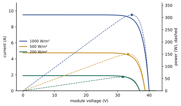
A solar cell is a large-area photodiode designed to deliver power. Sunlight creates electron-hole pairs, the junction field separates them, and the cell drives current through an external load. Its characteristic is the diode equation shifted by the light-generated current: \(I = I_{sc} - I_0(e^{V/(nV_T)} - 1)\). At short circuit it delivers its short-circuit current \(I_{sc}\), proportional to the light intensity; at open circuit its voltage \(V_{oc}\) is about 0.6 to 0.7 V per silicon cell; in between there is a maximum power point. Modules connect about 60 or 72 cells in series to reach useful voltages, and inverters use maximum power point tracking to keep operating at the best voltage as sunlight and temperature change.
import numpy as np

# Simple model of a 60-cell silicon module: I = Isc - I0 (exp(V / (Ns n Vt)) - 1)
Isc, Ns, n, Vt = 9.5, 60, 1.2, 0.0257          # amps, cells in series, ideality, thermal voltage (V)
Voc_target = 40.0                               # module open-circuit voltage (V)
I0 = Isc / (np.exp(Voc_target / (Ns * n * Vt)) - 1)

def current(V, G=1000.0):
    return (Isc * G / 1000.0) - I0 * (np.exp(V / (Ns * n * Vt)) - 1)

V = np.linspace(0, 42, 4201)
area = 1.7                                      # module area (m2)
for G in [1000.0, 500.0, 200.0]:
    I = np.clip(current(V, G), 0, None)
    P = V * I
    k = np.argmax(P)
    Voc = V[np.argmax(I <= 0)]
    print(f"Irradiance {G:6.0f} W/m2: Isc {I[0]:.2f} A, Voc {Voc:.1f} V, "
f"maximum power {P[k]:.0f} W at {V[k]:.1f} V and {I[k]:.2f} A, efficiency {P[k] / (G * area):.1%}")Irradiance 1000 W/m2: Isc 9.50 A, Voc 40.0 V, maximum power 311 W at 34.5 V and 9.02 A, efficiency 18.3% Irradiance 500 W/m2: Isc 4.75 A, Voc 38.7 V, maximum power 150 W at 33.3 V and 4.50 A, efficiency 17.6% Irradiance 200 W/m2: Isc 1.90 A, Voc 37.0 V, maximum power 57 W at 31.7 V and 1.80 A, efficiency 16.7%
At full sun the modeled module delivers about 310 W at 34.5 V, an efficiency of 18%, typical of panels a few years old (the best commercial panels now exceed 22%). The current, and so the power, falls almost in proportion to irradiance, while the voltage falls only slowly. Cell temperature matters too: silicon modules lose about 0.3 to 0.4% of their power per kelvin above 25 °C, so panels produce more on cold, clear days, a point in favor of solar power in Canada and the northern United States.
Transistors as switches
A transistor uses a small signal to control a large current. In a MOSFET (metal-oxide-semiconductor field-effect transistor), a voltage on an insulated gate creates an electric field that forms or removes a conducting channel between source and drain, so the device switches on with only a small on-resistance or off with almost no current, while the gate itself draws essentially no steady current. Billions of tiny MOSFETs switching between on and off represent the ones and zeros of digital logic in a processor. Large power MOSFETs and their cousins, IGBTs, switch hundreds of amperes thousands of times a second in motor drives, inverters, electric vehicle chargers and the switch-mode power supplies inside every computer.
Worked problem
Losses in a power switch
A MOSFET with an on-resistance of 10 mΩ switches a 10 A motor current. Find its conduction loss, and compare with a mechanical relay contact of 50 mΩ.
Show solution
- MOSFET: \(P = I^2R = 10^2 \times 0.010 = 1.0\) W.
- Relay contact: \(10^2 \times 0.050 = 5.0\) W.
Answer: The MOSFET dissipates 1 W while conducting, plus switching losses each time it turns on and off. It needs a heat sink, but it can switch thousands of times a second without wear, which no relay can; that is what makes variable-speed motor drives possible.
Sensors
Sensors turn physical quantities into electrical signals, and most rely on effects from this course:
- Temperature: resistance temperature detectors (RTDs) use the steady rise of a metal's resistance with temperature (a Pt100 RTD reads 100 Ω at 0 °C and about 138.5 Ω at 100 °C); thermistors use the large change of a semiconductor's resistance; thermocouples use the small voltage generated at a junction of two different metals.
- Magnetic field and current: in a Hall-effect sensor, the magnetic force on moving charge carriers (Lesson 7) pushes them to one side of a thin semiconductor strip, producing a transverse voltage \(V_H = IB/(nqt)\) proportional to the field. Hall sensors measure current without contact, detect the position of motor rotors and gear teeth, and sense wheel speed for anti-lock brakes.
- Force and strain: strain gauges in Wheatstone bridges (Lesson 6) and piezoelectric crystals, which generate charge when squeezed, measure loads, pressures and vibration.
- Light and proximity: photodiodes and image sensors, and capacitive sensors (Lesson 4) that detect a nearby finger, as in touchscreens, or the level of liquid in a tank.
Worked problem
A Hall-effect current sensor
A semiconductor Hall element 0.50 mm thick, with carrier density 1.0 × 10²¹ m⁻³, carries a 5.0 mA bias current. Find the Hall voltage in a 0.10 T field.
Show solution
- \(V_H = IB/(nqt) = (5.0 \times 10^{-3} \times 0.10)/(1.0 \times 10^{21} \times 1.6 \times 10^{-19} \times 5.0 \times 10^{-4})\).
- \(V_H = 5.0 \times 10^{-4}/0.080 = 6.3\) mV.
Answer: About 6 mV, easily amplified. Semiconductors are used rather than metals because their carrier density is millions of times lower, which makes the Hall voltage correspondingly larger. In a current sensor, a magnetic core concentrates the field of the measured conductor onto the Hall element, giving an isolated output proportional to current.
Common mistakes
MistakeTreating a diode as a resistor obeying Ohm's law.
InsteadDiode current rises exponentially with voltage; about 0.7 V is dropped when a silicon diode conducts.
MistakeForgetting diode drops and ripple in a rectifier calculation.
InsteadSubtract the diode drops from the peak and estimate ripple as I/(2fC) for full-wave.
MistakeExpecting a solar panel to give rated power in all conditions.
InsteadOutput scales with irradiance and falls at high cell temperature.
MistakeAssuming semiconductor resistance rises with temperature like a metal.
InsteadIntrinsic semiconductor conductivity increases with temperature.
MistakeIgnoring heat in power transistors.
InsteadConduction loss I²R_on and switching losses require heat sinking.
Summary and key terms
- Semiconductors have band gaps of about 1 to 3.5 eV; doping creates n-type (electron) and p-type (hole) material.
- A p-n junction conducts in one direction: I = I₀(e^(V/nV_T) − 1), with about 0.7 V forward drop in silicon.
- Rectifiers convert AC to DC; smoothing ripple is about I/(2fC) for full-wave.
- LED color is set by the band gap, λ ≈ 1240/E_g nm; photodiodes convert light to current.
- Solar cells deliver power at a maximum power point; output scales with irradiance and falls with temperature.
- MOSFETs switch large currents with small gate voltages; losses are I²R_on plus switching losses.
- Sensors use resistance, Hall, piezoelectric, photoelectric and capacitive effects.
- Band gap
- The energy separating the valence and conduction bands of a solid.
- Hole
- A missing electron in the valence band, acting as a positive charge carrier.
- Doping
- Adding impurities to a semiconductor to control its conductivity.
- Depletion region
- The carrier-free zone at a p-n junction with a built-in field.
- Diode
- A device that conducts current mainly in one direction.
- Rectifier
- A circuit that converts AC to DC.
- Light-emitting diode
- A junction that emits light when electrons and holes recombine.
- Maximum power point
- The operating point at which a solar cell delivers most power.
- MOSFET
- A field-effect transistor whose channel is controlled by an insulated gate voltage.
- Hall effect
- A transverse voltage across a current-carrying conductor in a magnetic field.
Practice problems
Work each problem on paper first, then reveal the answer to check.
What is the longest wavelength silicon can absorb (E_g = 1.12 eV)?
Show answer
1240/1.12 = 1107 nm.
What band gap gives an LED emitting at 620 nm?
Show answer
1240/620 = 2.0 eV.
A diode with I₀ = 10⁻¹² A and n = 1 is forward biased at 0.6 V. Estimate the current.
Show answer
10⁻¹² e^(0.6/0.0257) ≈ 1.4 × 10⁻² A (14 mA).
By what factor does that current rise if the voltage increases by 60 mV?
Show answer
e^(60/25.7) ≈ 10.
A 24 V RMS transformer feeds a bridge rectifier. Estimate the peak DC voltage.
Show answer
24√2 − 1.4 = 32.5 V.
What ripple results from 2 A, a full-wave rectifier and 10 000 µF at 60 Hz?
Show answer
2/(120 × 0.01) = 1.7 V.
A 400 W panel is rated at 25 °C. Estimate its output at 55 °C cell temperature (−0.35%/K).
Show answer
400 × (1 − 0.105) = 358 W.
Find the conduction loss of a MOSFET with 5 mΩ on-resistance carrying 30 A.
Show answer
4.5 W.
A Pt100 RTD has R = 100(1 + 0.00385T). Find R at 60 °C.
Show answer
123.1 Ω.
Why do Hall sensors use semiconductors rather than metals?
Show answer
The lower carrier density gives a much larger Hall voltage.
Lesson quiz · 5 questions
Score 60% or more to complete this lesson.
Create a free account to save your progress, take quizzes and earn a certificate.