
CMPUT-229 · Lesson 4 of 12 · 31 min
Digital logic for computer architects
A processor is a digital circuit: billions of transistors acting as switches, wired into gates, and gates wired into adders, multiplexers, registers and memories. You do not need to design transistors to understand computer organization, but you do need to know what the standard building blocks do, how fast they are and how they combine, because lesson 9 builds a RISC-V processor out of exactly these blocks. ROB-200 approached digital logic from the embedded-systems side, with logic levels, chips and microcontroller pins. This lesson takes the architect's view: Boolean algebra as a design tool, combinational circuits that compute, sequential circuits that remember, the arithmetic logic unit at the heart of the datapath, and the timing rules that set a processor's clock rate.
Boolean algebra
Digital logic works with two values, 0 and 1, and three basic operations: and (written as multiplication, A · B or AB), or (written A + B) and not (written with a bar or a prime, A′). Any function of binary inputs can be described by a truth table listing its output for every combination of inputs; a function of n inputs has 2ⁿ rows. Boolean algebra supplies identities for simplifying expressions, most of which resemble ordinary algebra: A + 0 = A, A · 1 = A, A · (B + C) = AB + AC. Some do not: A + A = A, A + 1 = 1, and A + BC = (A + B)(A + C).
The most useful identities for circuit design are De Morgan's laws: the complement of an and is the or of the complements, (AB)′ = A′ + B′, and the complement of an or is the and of the complements, (A + B)′ = A′B′. They let a designer move inversions around a circuit. They also show that a nand gate (and followed by not) or a nor gate is universal: any function can be built from nands alone, which is convenient because in CMOS technology nand and nor are the cheapest gates to build.
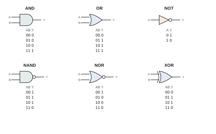
Any truth table can be turned into a circuit mechanically. Write one product term for each row whose output is 1, an and of every input, complemented where that input is 0, and or the terms together. The result, called the sum of products form, is often not the smallest circuit, but it always works, and it is the starting point for simplification. The program below derives the sum of products for the majority function, which is 1 when at least two of its three inputs are 1. Majority will reappear in a moment as the carry output of an adder.
from itertools import product

def majority(a, b, c):
    return int(a + b + c >= 2)

terms = []
print(' a b c | out')
for a, b, c in product((0, 1), repeat=3):
    y = majority(a, b, c)
    print(f' {a} {b} {c} |  {y}')
    if y:
        lits = [n if v else n + "'" for n, v in zip('abc', (a, b, c))]
        terms.append(''.join(lits))
print('sum of products:', ' + '.join(terms))
print('simplified     : ab + ac + bc')
# check the simplified form against the truth table
ok = all(majority(a, b, c) == ((a & b) | (a & c) | (b & c))
         for a, b, c in product((0, 1), repeat=3))
print('equivalent :', ok)a b c | out 0 0 0 | 0 0 0 1 | 0 0 1 0 | 0 0 1 1 | 1 1 0 0 | 0 1 0 1 | 1 1 1 0 | 1 1 1 1 | 1 sum of products: a'bc + ab'c + abc' + abc simplified : ab + ac + bc equivalent : True
The four product terms simplify to ab + ac + bc: three two-input ands and one three-input or. Designers once did such simplifications by hand with Karnaugh maps; today synthesis software performs them on circuits with millions of gates, but understanding the principle helps when reading hardware descriptions and when estimating cost.
Combinational building blocks
A combinational circuit's outputs depend only on its current inputs; it has no memory. Four combinational blocks appear again and again in processors. A decoder takes an n-bit input and turns on exactly one of its 2ⁿ outputs; it selects a register by number, or a memory row by address. A multiplexer, or mux, selects one of several inputs according to a control signal: a 2-to-1 mux outputs A when its select line is 0 and B when it is 1, computing S′A + SB. Muxes are everywhere in a datapath, choosing, for example, whether the ALU's second operand comes from a register or an immediate. An adder computes the sum of two binary numbers. And a comparator tests equality, which is just an xor of each bit pair followed by a nor of the results.
| Block | Inputs and outputs | Typical use in a processor |
|---|---|---|
| Decoder | n inputs, 2ⁿ outputs, exactly one active | Selecting a register or memory row |
| Multiplexer | k data inputs, log₂k select bits, one output | Choosing between register and immediate operands |
| Adder | Two n-bit numbers and a carry in; n-bit sum and carry out | The ALU, the PC + 4 incrementer, branch targets |
| Comparator | Two n-bit numbers; equal or less-than | Branch decisions |
| ALU | Two operands and an operation code; result and status | Executing arithmetic, logic and comparison instructions |
Adders
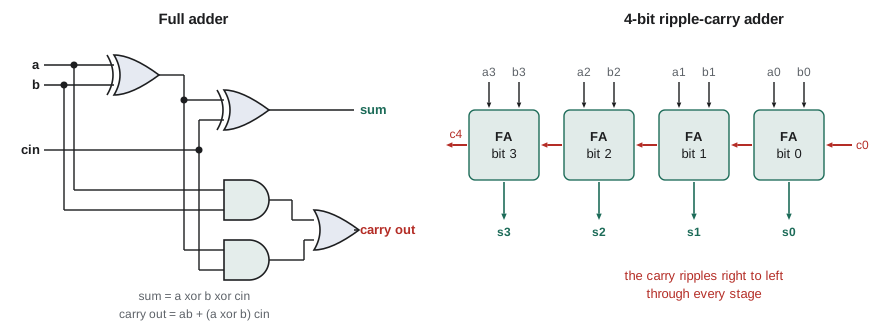
A half adder adds two bits, producing a sum bit (the xor of the inputs) and a carry bit (their and). A full adder adds three bits, two operand bits and an incoming carry, producing a sum s = a ⊕ b ⊕ cᵢₙ and a carry out cₒᵤₜ = ab + acᵢₙ + bcᵢₙ, which is exactly the majority function. Chaining n full adders, with each carry out feeding the next carry in, gives a ripple-carry adder for n-bit numbers. It is small, but slow: the carry may have to ripple through every stage, so the delay grows linearly with the width.
def full_adder(a, b, cin):
    """Return the sum bit and the carry out of one stage."""
    s = a ^ b ^ cin
    cout = (a & b) | (a & cin) | (b & cin)
    return s, cout

def ripple_add(x, y, bits=8, cin=0):
    carry, total, delay = cin, 0, 0
    for i in range(bits):
        s, carry = full_adder((x >> i) & 1, (y >> i) & 1, carry)
        total |= s << i
        delay += 2            # carry logic: one level of AND, one of OR
    return total, carry, delay

for x, y in [(23, 42), (200, 100), (255, 1)]:
    s, c, d = ripple_add(x, y)
    print(f'{x:3d} + {y:3d} = {s:3d} carry {c}  (worst-case carry path {d} gate delays)')
for bits in (8, 32, 64):
print(f'{bits}-bit ripple-carry adder: up to {2 * bits} gate delays')23 + 42 = 65 carry 0 (worst-case carry path 16 gate delays) 200 + 100 = 44 carry 1 (worst-case carry path 16 gate delays) 255 + 1 = 0 carry 1 (worst-case carry path 16 gate delays) 8-bit ripple-carry adder: up to 16 gate delays 32-bit ripple-carry adder: up to 64 gate delays 64-bit ripple-carry adder: up to 128 gate delays
Two gate delays per bit means 64 gate delays for a 32-bit add, far too slow for a processor whose whole cycle may allow only twenty or so. Fast adders compute the carries in parallel instead. For each bit position define generate \(g_i = a_i b_i\), meaning this position creates a carry by itself, and propagate \(p_i = a_i + b_i\), meaning it passes an incoming carry along. Then \(c_{i+1} = g_i + p_i c_i\), and by substituting repeatedly every carry can be written directly in terms of the g, p and the initial carry, in a fixed number of gate levels. Carry-lookahead and prefix adders organize this calculation as a tree, giving a delay that grows with the logarithm of the width. This is a recurring theme in hardware design: spend more gates to shorten the critical path.
def lookahead_carries(x, y, bits=4, c0=0):
    g = [(x >> i) & (y >> i) & 1 for i in range(bits)]
    p = [((x >> i) | (y >> i)) & 1 for i in range(bits)]
    c = [c0]
    for i in range(bits):
        c.append(g[i] | (p[i] & c[i]))     # expanded fully, each is two gate levels
    return g, p, c

g, p, c = lookahead_carries(0b1011, 0b0110)
print('generate  g3..g0:', g[::-1])
print('propagate p3..p0:', p[::-1])
print('carries   c4..c0:', c[::-1])
print('check: 11 + 6 =', 0b1011 + 0b0110, '= carry', c[4], 'and sum', (0b1011 + 0b0110) & 0xF)generate g3..g0: [0, 0, 1, 0] propagate p3..p0: [1, 1, 1, 1] carries c4..c0: [1, 1, 1, 0, 0] check: 11 + 6 = 17 = carry 1 and sum 1
The arithmetic logic unit
The ALU combines an adder with logic operations and selects among them with a multiplexer. A simple 1-bit ALU slice computes a and b, a or b and a full-adder sum for one bit position, and a mux chooses which result to output according to an operation code. Thirty-two slices side by side, with the carries chained, make a 32-bit ALU. Three tricks extend it. Subtraction comes free from two's complement: a − b = a + b′ + 1, so the ALU inverts b and sets the first carry in to 1. Set-less-than, the slt instruction, uses the subtractor: a < b exactly when a − b is negative, taking overflow into account, so the ALU outputs that sign as bit 0 and zeros elsewhere. And a zero detector, a nor of all 32 result bits, tells the branch logic whether two values were equal.
MASK = 0xFF                          # an 8-bit ALU keeps the output short

def alu(op, a, b):
    """8-bit ALU. ops: and, or, add, sub, slt (signed). Returns result and zero flag."""
    if op == 'and': r = a & b
    elif op == 'or': r = a | b
    elif op in ('add', 'sub', 'slt'):
        bb = (~b & MASK) if op != 'add' else b      # invert b to subtract
        cin = 1 if op != 'add' else 0               # ... and add 1
        r = (a + bb + cin) & MASK
        if op == 'slt':
            sa, sb, sr = a >> 7, b >> 7, r >> 7
            overflow = sa != sb and sr != sa
            r = sr ^ int(overflow)                  # true sign of a - b
    return r, int(r == 0)

def s8(x): return x - 256 if x & 0x80 else x
tests = [('and', 0b1100, 0b1010), ('or', 0b1100, 0b1010), ('add', 100, 27),
         ('sub', 27, 100), ('slt', 0x80, 0x01), ('slt', 0x01, 0x80), ('sub', 55, 55)]
for op, a, b in tests:
    r, z = alu(op, a, b)
print(f'{op:>3} {s8(a):5d} {s8(b):5d} -> {s8(r):5d} zero={z}')and 12 10 -> 8 zero=0 or 12 10 -> 14 zero=0 add 100 27 -> 127 zero=0 sub 27 100 -> -73 zero=0 slt -128 1 -> 1 zero=0 slt 1 -128 -> 0 zero=1 sub 55 55 -> 0 zero=1
Look at the two slt rows. As signed bytes, 0x80 is −128 and 0x01 is 1, so −128 < 1 gives 1 and 1 < −128 gives 0. Computing 0x80 − 0x01 overflows: the raw difference 0x7F has sign bit 0, which would wrongly say not less than. Correcting the sign with the overflow bit fixes it. The last row shows the zero output that a beq instruction would use.
Sequential circuits: storing bits
Combinational circuits cannot remember anything. To store a value, a circuit needs feedback: outputs fed back to inputs. The simplest storage element is a latch built from two cross-coupled nor or nand gates, which settles into one of two stable states and stays there. A D latch adds a data input D and an enable: while enabled, the output follows D; when disabled, it holds its last value. Processors mostly use D flip-flops, which change only at a clock edge, typically the moment the clock rises from 0 to 1. Between edges the output is stable, however the input changes. A register is a row of flip-flops sharing a clock, usually with a write-enable signal that decides whether the register loads a new value on the next edge.
The register file is the processor's fast local storage. RV32I has 32 registers, x0 to x31, each 32 bits wide. The register file is built so that two registers can be read and one written in every cycle, because most instructions read two source registers and write one destination. Reading uses two 32-input multiplexers controlled by the source register numbers; writing uses a 5-to-32 decoder to enable the one destination register. Register x0 is special: it is wired to always read as zero, and writes to it are ignored, which lets the ISA express many operations without extra instructions. For example, mv a0, a1 is really addi a0, a1, 0, and nop is addi x0, x0, 0.
class RegisterFile:
    """32 x 32-bit registers, two read ports, one write port, x0 hardwired to 0."""
    def __init__(self):
        self.r = [0] * 32
        self.pending = None
    def read(self, rs1, rs2):                  # combinational: available immediately
        return self.r[rs1], self.r[rs2]
    def write(self, rd, value, enable=True):    # takes effect at the clock edge
        self.pending = (rd, value & 0xFFFFFFFF) if enable else None
    def clock_edge(self):
        if self.pending and self.pending[0] != 0:
            rd, v = self.pending
            self.r[rd] = v
        self.pending = None

rf = RegisterFile()
rf.write(5, 1234)
print('before edge: x5 =', rf.read(5, 0)[0])
rf.clock_edge()
print('after edge : x5 =', rf.read(5, 0)[0])
rf.write(0, 99); rf.clock_edge()
print('after writing 99 to x0: x0 =', rf.read(0, 5)[0])before edge: x5 = 0 after edge : x5 = 1234 after writing 99 to x0: x0 = 0
Timing and the clock
Every gate takes time to switch, a few picoseconds in a modern chip, and signals take time to travel along wires. In a synchronous circuit, values leave flip-flops at a clock edge, pass through combinational logic, and must arrive at the next flip-flops early enough before the following edge. That margin is the setup time; the flip-flop also needs the input held steady for a short hold time after the edge. The longest delay through any combinational path between flip-flops is the critical path, and it sets the minimum clock period: the period must be at least the flip-flop's own output delay plus the critical path delay plus the setup time.
Worked problem
Finding the maximum clock rate
In a datapath, flip-flops have a clock-to-output delay of 30 ps and a setup time of 20 ps. The slowest path goes through a register file read (150 ps), a mux (25 ps), the ALU (200 ps) and another mux (25 ps). What is the maximum clock rate?
Show solution
- Critical path = 150 + 25 + 200 + 25 = 400 ps.
- Minimum period = 30 + 400 + 20 = 450 ps.
- Maximum clock rate = 1 / 450 ps ≈ 2.22 GHz.
Answer: About 2.2 GHz. To clock faster, the designer must shorten the critical path, for example with a faster adder, or split it across two cycles, which is what pipelining does in lesson 10.
This is the link between logic design and the performance equation of lesson 1. The clock period is set by the slowest path in the whole processor, so a single slow unit drags everything down. Designers therefore balance work so that no stage is much slower than the others, and they use the fast structures, such as carry-lookahead adders, on critical paths while saving area elsewhere.
Finite state machines
A sequential circuit with a register holding its current state and combinational logic computing the next state from the current state and inputs is a finite state machine, or FSM. FSMs control traffic lights, network interfaces, cache controllers and, in a multicycle processor, the sequence of steps that executes each instruction. In a Moore machine the outputs depend only on the state; in a Mealy machine they depend on the state and the inputs. The example below is a Moore machine that watches a serial bit stream and raises its output whenever the last three bits received were 1, 0, 1, a pattern detector of the kind used to find frame markers in communication links.
# States record how much of the pattern 1-0-1 has been seen so far.
NEXT = {            # (state, input bit) -> next state
    ('none', 0): 'none', ('none', 1): 'saw1',
    ('saw1', 0): 'saw10', ('saw1', 1): 'saw1',
    ('saw10', 0): 'none', ('saw10', 1): 'saw101',
    ('saw101', 0): 'saw10', ('saw101', 1): 'saw1',
}
OUTPUT = {'none': 0, 'saw1': 0, 'saw10': 0, 'saw101': 1}   # Moore outputs

state = 'none'
stream = [1, 0, 1, 0, 1, 1, 0, 0, 1, 0, 1]
outs = []
for bit in stream:                 # one clock edge per input bit
    state = NEXT[(state, bit)]
    outs.append(OUTPUT[state])
print('input :', ''.join(map(str, stream)))
print('output:', ''.join(map(str, outs)))
print('pattern found ending at positions', [i for i, o in enumerate(outs) if o])input : 10101100101 output: 00101000001 pattern found ending at positions [2, 4, 10]
Real processors are written not as gate diagrams but in hardware description languages such as Verilog, SystemVerilog or VHDL, or in newer languages such as Chisel, in which much of the open-source RISC-V hardware is written. A designer describes registers, combinational logic and state machines at roughly the level of this lesson, and synthesis tools turn the description into gates and then into a physical layout. Many free RISC-V cores can be read on the web and run on inexpensive field-programmable gate array (FPGA) boards, a good next step if this lesson interests you.
Common mistakes
MistakeThinking a ripple-carry adder is fast enough for a 32-bit processor.
InsteadIts delay grows linearly with width; real processors use carry-lookahead or prefix adders with logarithmic delay.
MistakeForgetting that subtraction needs both an inverted operand and a carry in of 1.
Insteada − b = a + b′ + 1; inverting b alone computes a − b − 1.
MistakeComputing slt from the sign of a − b alone.
InsteadIf the subtraction overflows, the sign is wrong; use the sign xor the overflow bit.
MistakeExpecting a register to change as soon as its input changes.
InsteadFlip-flop-based registers load only at the clock edge, and only when write-enabled.
MistakeAssuming the clock period depends on the average path delay.
InsteadIt is set by the critical path, the slowest path between flip-flops, plus flip-flop overheads.
Summary and key terms
- Any Boolean function can be written as a sum of products from its truth table; De Morgan's laws move inversions, and nand alone is universal.
- Decoders, multiplexers, adders and comparators are the combinational blocks of a datapath.
- A full adder computes s = a ⊕ b ⊕ c and carry = majority(a, b, c); chained, they form a ripple-carry adder with linear delay.
- Carry-lookahead adders compute carries in parallel from generate and propagate signals, with logarithmic delay.
- An ALU selects among logic and arithmetic results; subtraction adds the inverted operand plus 1, and slt uses the corrected sign of a − b.
- Flip-flops store bits and change only at clock edges; the register file provides two reads and one write per cycle, with x0 fixed at zero.
- The clock period must cover clock-to-output delay, the critical path and setup time; finite state machines combine a state register with next-state logic.
- Truth table
- A table listing a Boolean function's output for every combination of inputs.
- Sum of products
- An or of and terms, one for each truth-table row whose output is 1.
- Multiplexer
- A circuit that selects one of several inputs according to select signals.
- Full adder
- A circuit adding two bits and a carry in to produce a sum bit and a carry out.
- Carry lookahead
- Computing carries in parallel from generate and propagate signals instead of letting them ripple.
- ALU
- Arithmetic logic unit: the combinational circuit that performs arithmetic, logic and comparison operations.
- D flip-flop
- A storage element that captures its input at a clock edge and holds it until the next edge.
- Register file
- The set of processor registers, with read and write ports.
- Critical path
- The longest combinational delay between storage elements, which limits the clock rate.
- Finite state machine
- A sequential circuit whose next state depends on its current state and inputs.
Practice problems
Work each problem on paper first, then reveal the answer to check.
Write the sum of products for the xor of a and b.
Show answer
a'b + ab'.
Use De Morgan's law to rewrite (A + B + C)′.
Show answer
A′B′C′.
How many select bits does an 8-to-1 multiplexer need?
Show answer
Three, since 2³ = 8.
Compute the sum and carry out of a full adder with a = 1, b = 1, cin = 1.
Show answer
Sum 1 (1 ⊕ 1 ⊕ 1) and carry 1 (majority).
With 2 gate delays per bit, what is the worst-case delay of a 16-bit ripple-carry adder?
Show answer
32 gate delays.
For bits a = 1, b = 0, what are generate and propagate?
Show answer
g = 0 (not both 1) and p = 1 (at least one 1), so an incoming carry is passed on.
How does an ALU compute 7 − 9 with an adder?
Show answer
It adds 7 to the inverted bits of 9 with carry in 1, which is 7 + (−9), giving −2.
Why does RISC-V hardwire x0 to zero?
Show answer
A permanent zero lets many operations, such as mv, nop, neg and comparisons with zero, use existing instructions.
A path has 300 ps of logic, flip-flops need 25 ps clock-to-output and 15 ps setup. What is the maximum clock rate?
Show answer
1 / 340 ps ≈ 2.94 GHz.
What distinguishes a Moore machine from a Mealy machine?
Show answer
Moore outputs depend only on the state; Mealy outputs depend on the state and the current inputs.
Lesson quiz · 5 questions
Score 60% or more to complete this lesson.
Create a free account to save your progress, take quizzes and earn a certificate.