
ELE-202 · Lesson 8 of 12 · 40 min
Operational amplifiers
The operational amplifier, or op amp, is the most widely used analog building block in electronics. It is an integrated circuit containing dozens of transistors, but engineers rarely need to think about them. From the outside, an op amp is a very high-gain amplifier of the difference between two input voltages, and with a few resistors around it, it becomes an amplifier of almost any precise gain, a buffer, a summer, a subtractor, a filter, or a converter from current to voltage. The name comes from its original use in analog computers in the 1940s, where op amps performed mathematical operations such as addition and integration.
Op amps appear in every sensor interface, audio system, power supply controller, battery management system and measurement instrument. Inside a data center they condition the signals from temperature, current and pressure sensors, and in optical receivers a close relative, the transimpedance amplifier, converts the tiny photodiode current from a fiber into a voltage. This chapter introduces the ideal op amp model, works through the standard circuits with the methods of Lessons 2 and 4, and explains the practical limits of real devices.
The op amp and its model
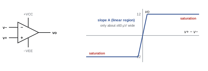
An op amp has two inputs, the non-inverting input (marked +) and the inverting input (marked −), and one output. It also has two power supply connections, often \(+V_{CC}\) and \(-V_{EE}\) (for example ±15 V), or a single supply and ground, which are usually left off circuit diagrams but are always there. The output voltage is measured relative to ground.
An op amp amplifies the difference between its inputs:
where \(A\) is the open-loop gain, typically \(10^5\) to \(10^6\) or more. The output cannot exceed the supply voltages: when the formula asks for more, the output saturates at a level near the supply rail (within a volt or two for older designs, within millivolts for "rail-to-rail" designs). The resulting transfer characteristic has a very steep linear region and two flat saturation regions.
Worked problem
How small is the linear region?
An op amp has an open-loop gain of 200,000 and saturates at ±12 V. What input difference drives it into saturation?
Show solution
- \(v_+ - v_- = v_o/A = 12/200{,}000 = 6 \times 10^{-5}\) V.
Answer: Just 60 µV. Without feedback, any practical signal saturates the output, so an op amp used open-loop is only useful as a comparator (an output that switches high or low depending on which input is larger). For linear amplification, op amps are always used with negative feedback.
The ideal op amp
With negative feedback, a path from the output back to the inverting input, the enormous gain works for us. The output settles at whatever voltage makes \(v_+ - v_-\) almost exactly zero, because any difference is amplified \(A\) times and corrected. This leads to the ideal op amp model, which predicts real op-amp circuits accurately in most applications:
- Rule 1, no input current: the inputs draw no current, \(i_+ = i_- = 0\) (real input currents are nanoamperes or picoamperes).
- Rule 2, virtual short: with negative feedback, the two input voltages are equal, \(v_+ = v_-\). The inputs are not actually connected (no current flows between them), which is why it is called a "virtual" short.
- The output can supply whatever current the circuit needs (within limits), so its output resistance is effectively zero.
Analysis of an ideal op amp circuit uses only these rules plus KCL at the input nodes. One warning: never write KCL at the op amp's output node. The output current comes from the power supplies through pins not shown on the diagram, so it is unknown and KCL there gives no useful information.
The inverting amplifier
In the inverting amplifier, the input signal drives the inverting input through a resistor \(R_1\), a feedback resistor \(R_f\) connects the output back to the inverting input, and the non-inverting input is grounded.
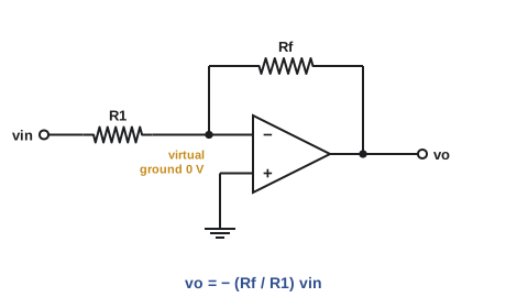
By the virtual short, \(v_- = v_+ = 0\): the inverting input is a virtual ground. The current through \(R_1\) is \(v_{in}/R_1\). Since no current enters the op amp, all of it flows through \(R_f\), producing a drop of \(R_f v_{in}/R_1\) from the inverting input (0 V) to the output. So:
The gain depends only on the ratio of two resistors, not on the op amp's own gain, which varies from part to part and with temperature. That is the magic of negative feedback: precise, stable gain from an imprecise amplifier. The minus sign means the output is inverted. The input resistance seen by the source is simply \(R_1\), because the inverting input sits at 0 V.
Worked problem
An inverting amplifier
An inverting amplifier has \(R_1 = 10\) kΩ and \(R_f = 47\) kΩ, with ±15 V supplies. Find the gain, the output for \(v_{in} = 0.5\) V, the input current and the input resistance.
Show solution
- Gain \(= -R_f/R_1 = -4.7\).
- \(v_o = -4.7 \times 0.5 = -2.35\) V, well within the supply limits.
- Input current \(= 0.5/10{,}000 = 50\) µA, which also flows through \(R_f\): \(50\) µA × 47 kΩ = 2.35 V drop. ✓
- Input resistance \(= R_1 = 10\) kΩ.
Answer: Gain −4.7, output −2.35 V, input current 50 µA and input resistance 10 kΩ.
The non-inverting amplifier and the voltage follower
In the non-inverting amplifier, the signal drives the non-inverting input directly, and the feedback network \(R_f\) and \(R_1\) forms a divider from the output to ground, with its midpoint at the inverting input.
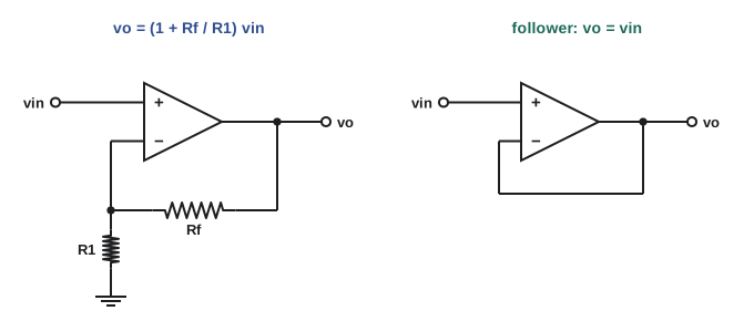
The divider gives \(v_- = v_o R_1/(R_1 + R_f)\), and the virtual short sets \(v_- = v_{in}\). Solving:
The gain is positive and at least 1. Because the input drives the op amp input directly and draws no current, the input resistance is essentially infinite, so the amplifier does not load the source at all.
Setting \(R_f = 0\) and removing \(R_1\) gives the voltage follower (buffer): the output is connected straight to the inverting input, and \(v_o = v_{in}\). A gain of 1 sounds useless, but the follower draws no current from its source and can drive a heavy load from its low-resistance output. It is the cure for the loading problem of Lesson 2.
Worked problem
Curing the loaded divider
In Lesson 2, a divider of two 10 kΩ resistors across 24 V delivered only 8 V to a 10 kΩ sensor input instead of 12 V. What does the sensor receive if a voltage follower is placed between the divider and the sensor?
Show solution
- The follower's input draws no current, so the divider is unloaded and its midpoint stays at \(24 \times 10/20 = 12\) V.
- The follower output equals its input: 12 V.
- The op amp output supplies the sensor's current, \(12/10{,}000 = 1.2\) mA, from its power supply, not from the divider.
Answer: 12 V. The buffer isolates the divider from the load, a pattern used throughout electronics.
Worked problem
Non-inverting gain and saturation
A non-inverting amplifier has \(R_1 = 10\) kΩ and \(R_f = 30\) kΩ and is supplied from ±12 V (saturating near ±12 V). Find the output for inputs of 2 V and 4 V.
Show solution
- Gain \(= 1 + 30/10 = 4\).
- 2 V input: \(v_o = 8\) V, within range.
- 4 V input: the formula gives 16 V, beyond the supply. The output saturates near +12 V, and the virtual-short rule no longer holds.
Answer: 8 V for a 2 V input; for 4 V the output clips at about +12 V. Always check that the predicted output lies within the supply limits.
Summing and difference amplifiers
The summing amplifier
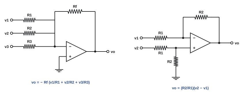
Connecting several inputs, each through its own resistor, to the virtual ground of an inverting amplifier adds their currents. KCL at the inverting input (at 0 V) gives:
Each input is weighted by its own resistor, and because the summing point is a virtual ground, the inputs do not interact. Audio mixing consoles combine channels this way. With binary-weighted resistors, a summing amplifier becomes a simple digital-to-analog converter.
Worked problem
A 3-bit digital-to-analog converter
A summing amplifier has \(R_f = 10\) kΩ and inputs through \(R_1 = 10\) kΩ (most significant bit), \(R_2 = 20\) kΩ and \(R_3 = 40\) kΩ (least significant bit). Each input is 1 V for a binary 1 and 0 V for a 0. Find the output for the codes 111, 101 and 001.
Show solution
- Weights: \(R_f/R_1 = 1\), \(R_f/R_2 = 0.5\), \(R_f/R_3 = 0.25\).
- 111: \(v_o = -(1 + 0.5 + 0.25) = -1.75\) V.
- 101: \(v_o = -(1 + 0 + 0.25) = -1.25\) V.
- 001: \(v_o = -0.25\) V.
Answer: −1.75 V, −1.25 V and −0.25 V: the output is proportional to the binary number (7, 5 and 1) in steps of −0.25 V. Real converters use more precise structures, but the principle is the same.
The difference amplifier
Many sensors produce a small signal riding on a large common voltage, for example the two midpoints of a Wheatstone bridge, each at about half the supply voltage. The difference amplifier responds only to the difference. With \(v_1\) driving the inverting input through \(R_1\) (feedback \(R_2\)), and \(v_2\) driving the non-inverting input through a matching divider of \(R_1\) and \(R_2\) to ground:
The voltage common to both inputs is rejected. The quality of that rejection, the common-mode rejection ratio (CMRR), depends on how well the resistor ratios match: a 0.1% mismatch can let a little of the common voltage through. Instrumentation amplifiers, which add input buffers to a difference amplifier, give very high input resistance and excellent rejection and are the standard front end for bridge sensors, strain gauges and thermocouples.
Worked problem
Amplifying a bridge signal
A strain-gauge bridge produces 2.05 V and 2.00 V at its two midpoints. A difference amplifier with \(R_2/R_1 = 10\) amplifies them. What is the output, and what would an amplifier that also passed the common voltage produce?
Show solution
- Difference: \(2.05 - 2.00 = 0.05\) V.
- \(v_o = 10 \times 0.05 = 0.5\) V.
- A non-inverting amplifier of gain 10 on the 2.05 V point alone would try to output 20.5 V and saturate; the useful 50 mV would be swamped by the 2 V common level.
Answer: 0.5 V, representing only the strain signal. Rejecting the common-mode voltage is the whole purpose of the difference amplifier.
Current to voltage: the transimpedance amplifier
Some sensors produce a current rather than a voltage. A photodiode, for example, produces a current proportional to the light falling on it. Feeding that current into the virtual ground of an op amp with only a feedback resistor gives \(v_o = -i_{in}R_f\). The gain has units of ohms (volts per ampere), hence the name transimpedance amplifier (TIA). A photodiode current of 2 µA into a 1 MΩ feedback resistor gives −2 V. Every optical transceiver in a data center network has a high-speed transimpedance amplifier immediately behind its photodiode, converting microamperes of photocurrent into a voltage that the receiver can decode.
Analyzing op amp circuits systematically
More complex op amp circuits are analyzed with nodal analysis plus the two ideal rules. Write KCL at the op amp input nodes (using \(i_+ = i_- = 0\)) and at any other nodes, use \(v_+ = v_-\) as an extra equation, and never write KCL at an op amp output. Cascaded stages can be analyzed one at a time, because each ideal op amp output is a voltage source unaffected by what it drives: the overall gain is the product of the stage gains.
Worked problem
A two-stage cascade
A non-inverting stage with gain 4 is followed by an inverting stage with gain −2. The input is 0.5 V and the supplies are ±12 V. Find each stage's output.
Show solution
- Stage 1: \(4 \times 0.5 = 2\) V.
- Stage 2: \(-2 \times 2 = -4\) V.
- Overall gain: \(4 \times (-2) = -8\). Both outputs are within ±12 V.
Answer: 2 V after stage 1 and −4 V at the output, an overall gain of −8. If the input rose above 1.5 V, stage 2 would saturate at about −12 V.
Real op amps
The ideal model is accurate when the circuit gain is far below the open-loop gain and the signals are slow. Real op amps depart from it in several ways; Lesson 9 quantifies the DC errors, and later courses explore the rest:
- Finite open-loop gain. For a non-inverting amplifier with feedback fraction \(\beta = R_1/(R_1 + R_f)\), the exact gain is \(A/(1 + A\beta)\). With \(A = 200{,}000\) and an ideal gain of 4 (\(\beta = 0.25\)), the exact gain is 3.99992, an error of 0.002%. The ideal rules are excellent here.
- Limited bandwidth. Open-loop gain falls with frequency. Many op amps have a roughly constant gain-bandwidth product: a 1 MHz op amp used at a gain of 4 has a bandwidth of about 250 kHz.
- Slew rate. The output can change only so fast (for example 0.5 V/µs for older general-purpose parts), which distorts large, fast signals.
- Offsets and bias currents. Small built-in input voltage offsets (microvolts to millivolts) and input currents (picoamperes to nanoamperes) produce output errors, important in precision measurement.
- Output limits. The output saturates near the supply rails and can only supply limited current, typically tens of milliamperes.
Datasheets specify all of these, and choosing an op amp means matching them to the application: precision and low offset for sensors, high bandwidth and slew rate for video and communications, low power for battery devices.
Common mistakes
MistakeWriting KCL at the op amp's output node.
InsteadThe output current comes from the power supply and is unknown; write KCL only at the inputs and other nodes.
MistakeApplying the virtual short to an op amp without negative feedback.
InsteadWithout negative feedback (comparators, or saturated outputs), \(v_+ \ne v_-\) in general.
MistakePredicting outputs beyond the supply voltages.
InsteadCheck every output against the supply limits; beyond them the op amp saturates.
MistakeMixing up the inverting and non-inverting gain formulas.
InsteadInverting: \(-R_f/R_1\). Non-inverting: \(1 + R_f/R_1\).
MistakeAssuming the inverting amplifier has high input resistance.
InsteadIts input resistance is \(R_1\); use a non-inverting stage or follower when the source must not be loaded.
Summary and key terms
- An op amp amplifies \(v_+ - v_-\) by a huge open-loop gain \(A\); its output saturates near the supply rails.
- With negative feedback, the ideal rules apply: no input current and \(v_+ = v_-\) (virtual short).
- Inverting amplifier: \(v_o = -(R_f/R_1)v_{in}\), input resistance \(R_1\), virtual ground at the inverting input.
- Non-inverting amplifier: \(v_o = (1 + R_f/R_1)v_{in}\), very high input resistance; the voltage follower has gain 1 and buffers loads.
- Summing amplifier: \(v_o = -R_f\sum v_k/R_k\). Difference amplifier: \(v_o = (R_2/R_1)(v_2 - v_1)\), rejecting common-mode voltage.
- Transimpedance amplifier: \(v_o = -i_{in}R_f\), used with photodiodes in optical receivers.
- Analyze with KCL at input nodes and the virtual short; never KCL at an output; cascaded gains multiply.
- Real op amps have finite gain, limited bandwidth and slew rate, offsets, and output limits.
- Operational amplifier
- A high-gain differential amplifier integrated circuit used with external feedback components.
- Open-loop gain
- The op amp's own gain \(A\) without feedback, typically \(10^5\) or more.
- Negative feedback
- Returning part of the output to the inverting input so the amplifier corrects its own errors.
- Saturation
- The condition in which the output is limited near a supply rail and no longer follows the input.
- Virtual short
- The near-equality of the two input voltages of an op amp with negative feedback.
- Virtual ground
- An inverting input held at 0 V by feedback when the non-inverting input is grounded.
- Inverting amplifier
- An op amp circuit with gain \(-R_f/R_1\).
- Non-inverting amplifier
- An op amp circuit with gain \(1 + R_f/R_1\) and very high input resistance.
- Voltage follower
- A unity-gain buffer that isolates a source from a load.
- Summing amplifier
- An op amp circuit whose output is a weighted sum of several inputs.
- Difference amplifier
- An op amp circuit that amplifies the difference between two inputs.
- Common-mode rejection
- An amplifier's ability to ignore voltage common to both inputs.
- Transimpedance amplifier
- An op amp circuit converting an input current to an output voltage.
- Comparator
- A circuit whose output switches high or low depending on which input is larger.
- Gain-bandwidth product
- The roughly constant product of closed-loop gain and bandwidth for many op amps.
- Slew rate
- The maximum rate of change of an op amp's output voltage.
Practice problems
Work each problem on paper first, then reveal the answer to check.
An op amp with \(A = 10^5\) has \(v_+ = 2.00010\) V and \(v_- = 2.00000\) V, with ±15 V supplies. What is the output?
Show answer
A × 0.1 mV = 10 V, within the supplies.
Design an inverting amplifier with a gain of −20 and an input resistance of 5 kΩ.
Show answer
R₁ = 5 kΩ, R_f = 100 kΩ.
An inverting amplifier has \(R_1 = 2.2\) kΩ and \(R_f = 22\) kΩ. Find the output for \(v_{in} = -0.3\) V.
Show answer
Gain −10, so v_o = +3 V.
Design a non-inverting amplifier with a gain of 11 using a 1 kΩ resistor for \(R_1\).
Show answer
R_f = (11 − 1) × 1 kΩ = 10 kΩ.
A non-inverting amplifier with gain 6 runs from ±9 V supplies (saturating at ±9 V). What is the largest input it can amplify linearly?
Show answer
9/6 = 1.5 V (in magnitude).
A summing amplifier has \(R_f = 20\) kΩ, inputs of 0.5 V through 10 kΩ and −1.0 V through 40 kΩ. Find \(v_o\).
Show answer
v_o = −20k(0.5/10k − 1.0/40k) = −20k(50 µA − 25 µA) = −0.5 V.
A difference amplifier with \(R_2/R_1 = 50\) receives 1.512 V and 1.500 V (with the larger on the non-inverting side). Find the output.
Show answer
50 × 0.012 = 0.6 V.
A photodiode produces 0.5 µA. What feedback resistor gives a 1 V output magnitude in a transimpedance amplifier?
Show answer
R_f = 1/(0.5 × 10⁻⁶) = 2 MΩ.
Using the exact formula \(A/(1 + A\beta)\), what is the gain of an ideal-gain-of-100 non-inverting amplifier with \(A = 10^5\)?
Show answer
β = 0.01; gain = 10⁵/(1 + 1000) = 99.9, an error of 0.1%.
An op amp has a gain-bandwidth product of 10 MHz. What bandwidth can you expect at a closed-loop gain of 50?
Show answer
About 10 MHz/50 = 200 kHz.
Lesson quiz · 5 questions
Score 60% or more to complete this lesson.
Create a free account to save your progress, take quizzes and earn a certificate.